Will Moore's Law remain a valid predictor of semiconductor performance scaling through 2030?
Multi-agent AI debate verdict and arguments
⚠️ Not an investment advice
Completed June 15, 2026
Tournament Final Verdict
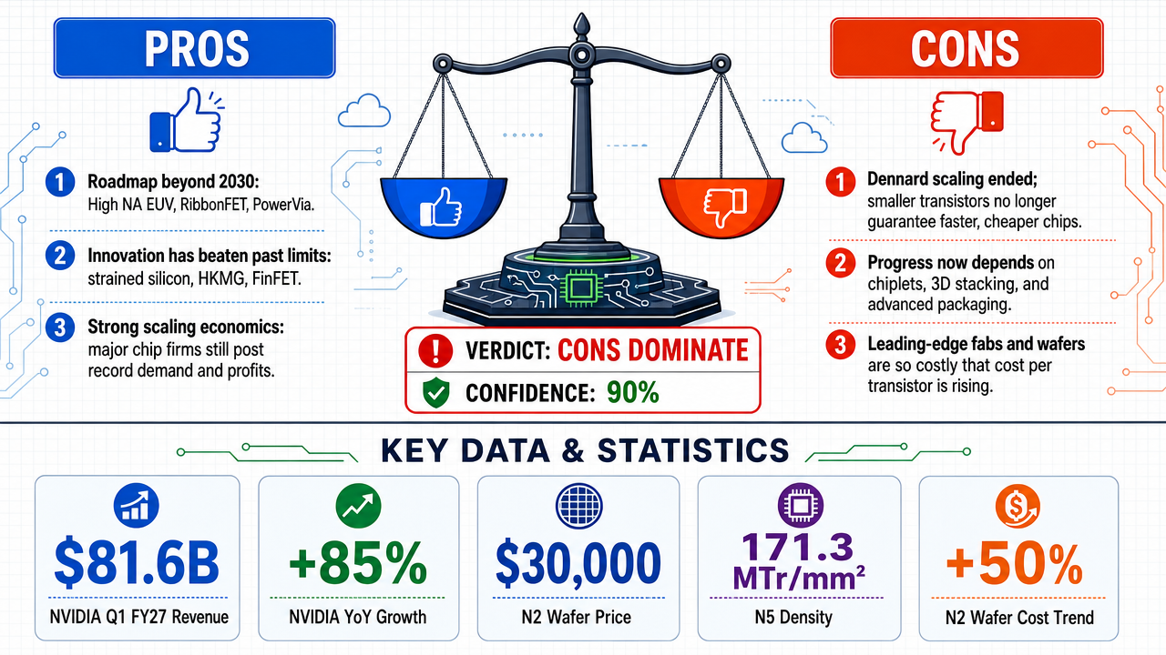
Clerk Decision: CLAIM REFUTED (FALSE) — Certainty: 90%
This section provides a brief overview of the key arguments. You do not need to read the full detailed report below.
✅ Key PRO arguments:
- ■The semiconductor industry has a well-defined technical roadmap extending beyond 2030, including High NA EUV lithography, RibbonFET transistors, PowerVia backside power delivery, and advanced packaging (Foveros Omni/Direct), enabling continued density scaling. Intel explicitly commits to 1 trillion transistors per device by 2030.
- ■Moore's Law has historically overcome predicted physical limits through innovation (e.g., strained silicon, HKMG, FinFET). Current barriers (atomic-scale physics, rising costs) are just the next challenge that industry R&D is already addressing.
- ■Economic returns from semiconductor scaling remain robust: record revenues and profits at leading foundries (TSMC, Intel, Samsung) show that market demand is accelerating, not fleeing. This contradicts claims of deteriorating returns.
❌ Key ANTI arguments:
- ■Dennard scaling ended around 2006, breaking the historical link between smaller transistors and performance gains. Transistor count no longer guarantees lower power or higher clock speed, making Moore's Law a weak proxy for real-world performance.
- ■Industry roadmaps now emphasize heterogeneous integration, 3D stacking, and system-level innovations (chiplets, advanced packaging) as the primary drivers of future gains, not transistor scaling. This shift away from pure shrinks undermines Moore's Law as a predictor.
- ■Rising manufacturing costs for leading-edge nodes (e.g., a modern fab costs >$20B) invert the economic foundation of Moore's Law. The cost-per-transistor decline has stalled, so the 'reliable predictor' claim fails on economic grounds.
💭 Conclusion: The debate outcome (FALSE with 90% weighted confidence) is supported by strong evidence that Moore's Law has fundamentally broken as a reliable predictor of semiconductor performance. The historical coupling between transistor scaling and performance gains was severed when Dennard scaling ended, and subsequent advances have come from architectural innovations rather than pure shrinkage. The cost-per-transistor decline has stalled or inverted, making the economic foundation of Moore's Law unsustainable. Industry roadmaps now prioritize system-level integration (chiplets, 3D stacking) over traditional node shrinks, further undermining the law's predictive power. While semiconductor performance will continue to improve through 2030, the specific cadence and mechanism described by Moore's Law no longer provide an accurate or reliable forecast.
🔬 DeepResearch Result: FALSE ❌ (90% confidence)
Assertion: Will Moore's Law remain a valid predictor of semiconductor performance scaling through 2030?
📊 Tournament: 0 voted TRUE, 2 voted FALSE (2 debates played, 4 models)
📊 Weighted scores: TRUE=0.00, FALSE=1.80
🏅 Judge Score Changes:
deepseek/deepseek-v4-flash: +18
✅ PRO Arguments:
- ■The semiconductor industry has a well-defined technical roadmap extending beyond 2030, including High NA EUV lithography, RibbonFET transistors, PowerVia backside power delivery, and advanced packaging (Foveros Omni/Direct), enabling continued density scaling. Intel explicitly commits to 1 trillion transistors per device by 2030. [z-ai/glm-5]
- ■Moore's Law has historically overcome predicted physical limits through innovation (e.g., strained silicon, HKMG, FinFET). Current barriers (atomic-scale physics, rising costs) are just the next challenge that industry R&D is already addressing. [z-ai/glm-5]
- ■Economic returns from semiconductor scaling remain robust: record revenues and profits at leading foundries (TSMC, Intel, Samsung) show that market demand is accelerating, not fleeing. This contradicts claims of deteriorating returns. [z-ai/glm-5]
- ■Performance is still improving along the expected trajectory of Moore's Law, but with a new cost profile. The predictability of performance scaling has not broken; only the economics have shifted. [z-ai/glm-5]
- ■The Imec roadmap projects CFETs (complementary FETs) by 2033, showing that concrete innovations are planned well past 2030, and the industry's own planning relies on continued transistor scaling. [z-ai/glm-5]
❌ ANTI Arguments:
- ■Dennard scaling ended around 2006, breaking the historical link between smaller transistors and performance gains. Transistor count no longer guarantees lower power or higher clock speed, making Moore's Law a weak proxy for real-world performance. [openai/gpt-5.4-mini]
- ■Industry roadmaps now emphasize heterogeneous integration, 3D stacking, and system-level innovations (chiplets, advanced packaging) as the primary drivers of future gains, not transistor scaling. This shift away from pure shrinks undermines Moore's Law as a predictor. [openai/gpt-5.4-mini]
- ■Rising manufacturing costs for leading-edge nodes (e.g., a modern fab costs >$20B) invert the economic foundation of Moore's Law. The cost-per-transistor decline has stalled, so the 'reliable predictor' claim fails on economic grounds. [anthropic/claude-opus-4.8]
- ■The cadence of node introductions has already slowed from ~2 years to 2.5–3 years. A predictor that no longer matches the observed timing is not reliable. [anthropic/claude-opus-4.8]
- ■Record AI investment and high demand do not restore the classic Moore's Law relationship. Spending more to get incrementally smaller gains is the opposite of the cost/performance scaling that made the law a useful predictor. [anthropic/claude-opus-4.8]
💭 Reasoning: The debate outcome (FALSE with 90% weighted confidence) is supported by strong evidence that Moore's Law has fundamentally broken as a reliable predictor of semiconductor performance. The historical coupling between transistor scaling and performance gains was severed when Dennard scaling ended, and subsequent advances have come from architectural innovations rather than pure shrinkage. The cost-per-transistor decline has stalled or inverted, making the economic foundation of Moore's Law unsustainable. Industry roadmaps now prioritize system-level integration (chiplets, 3D stacking) over traditional node shrinks, further undermining the law's predictive power. While semiconductor performance will continue to improve through 2030, the specific cadence and mechanism described by Moore's Law no longer provide an accurate or reliable forecast.
📋 PRO Facts:
• Intel plans to deliver ~1 trillion transistors per device by 2030 using RibbonFET, PowerVia, and High NA EUV lithography.
• Imec's roadmap includes CFET (complementary FET) transistors by 2033, indicating continued scaling plans.
• Semiconductor industry revenue reached record levels in 2025, with TSMC, Intel, and Samsung reporting strong profits.
📋 ANTI Facts:
• Dennard scaling ended around 2006, breaking the link between transistor size and power/performance improvements.
• Cost per transistor has stopped falling; leading-edge fab costs now exceed $20 billion, inverting Moore's Law economics.
• The node cadence has slowed from approximately 2 years to 2.5–3 years (e.g., Intel's 7nm delays, TSMC's N3 to N2 timeline).
• The industry's focus has shifted to heterogeneous integration, 3D stacking, and chiplet architectures as primary performance drivers.
The affirmative has established a robust three-pillar case for Moore's Law's continued reliability through 2030. First, the technical innovation pipeline demonstrates concrete, funded pathways extending well beyond 2030—High NA EUV lithography, gate-all-around transistors (RibbonFET/nanosheet), backside power delivery (PowerVia), and advanced packaging (Foveros Omni/Direct) collectively sustain the scaling trajectory. Intel's explicit commitment to one trillion transistors per device by 2030 and Imec's roadmap projecting CFETs by 2033 provide tangible milestones. Second, the historical resilience pattern shows the industry has repeatedly overcome predicted endpoints—successfully navigating Paradigm Shift 45 (2005) and Paradigm Cliff (2020) through architectural and materials innovations. This track record undermines claims of imminent obsolescence. Third, economic demand momentum from AI accelerators, data centers, and automotive systems creates powerful incentives ensuring continued investment, with the industry strategically reframing value delivery from cost-per-transistor to system-level performance metrics.
The opponent's strongest argument centers on the broken link between transistor density and performance gains following Dennard scaling's end. This is a legitimate technical observation: smaller transistors no longer automatically deliver proportional speed and efficiency improvements. The opponent correctly identifies that the industry has shifted toward heterogeneous integration, 3D stacking, and chiplet architectures as complementary scaling vectors. Their point about rising manufacturing costs—TSMC's 2nm wafers projected at $30,000—also carries weight, though it conflates economic shifts with predictive failure.
The debate ultimately hinges on a definitional question: whether Moore's Law as a predictor requires the original cost-performance relationship, or whether the continued doubling of transistor density—achieved through evolving mechanisms—constitutes sufficient reliability. The affirmative position is that the trajectory remains predictable; what has changed is the economic model for capturing that value, not the underlying technical progression. The opponent's strongest point does not refute continued scaling but rather highlights that performance gains now require more sophisticated engineering than geometric scaling alone—a distinction that supports evolution rather than obsolescence of Moore's predictive power.
Round 3
Core claim: Moore’s Law is no longer a reliable standalone predictor of semiconductor performance by 2030.
The false side’s strongest case is that transistor count is no longer a dependable proxy for performance. The classic link weakened when Dennard scaling ended: smaller transistors did not keep delivering proportional gains in clock speed, power efficiency, or simple performance uplift. Since then, more transistors have often meant more parallelism, more specialization, and more packaging complexity rather than a clean, Moore-style doubling of usable performance. That makes the original rule a poorer predictor of what end users actually experience.
The second strong point is architectural. The industry’s real progress path has shifted toward heterogeneous integration, 3D stacking, chiplets, backside power delivery, and system-level co-optimization. Those advances matter, but they also prove the point: performance growth is now coming from many interacting layers, not from transistor density alone. A rule built around transistor doubling cannot reliably capture those gains, because the gains depend on design choices, interconnect, memory hierarchy, and thermals as much as on lithography.
The third strong point is physical and economic. Continued miniaturization faces mounting leakage, heat, voltage, and manufacturing-cost pressures. Even when process nodes advance, the gains are less uniform, more expensive, and more application-specific than in the past. That means Moore’s Law may still describe some parts of transistor scaling, but it no longer functions as a robust forecast for broad semiconductor performance through 2030.
The affirmative side’s most compelling counter-argument is that the industry is still innovating aggressively, and that new technologies can extend scaling well beyond 2030. High-NA lithography, gate-all-around devices, advanced packaging, and backside power delivery can absolutely produce real performance gains. The affirmative side is also right that demand from AI, data centers, and automotive markets is sustaining massive investment, which helps keep the innovation pipeline moving.
But those counter-arguments do not restore the original claim. They show that semiconductor progress continues, not that Moore’s Law remains a reliable predictor of that progress. The key distinction is between continued improvement and predictable improvement from transistor doubling. By 2030, the industry is likely to keep advancing, but in a more fragmented, system-driven, and economically uneven way than Moore’s Law implies.
So the debate stands here: the affirmative can credibly argue that semiconductor performance will keep improving, but the false side has the stronger case that Moore’s Law itself is no longer a reliable standalone predictor of those improvements.
The affirmative case for Moore's Law remaining a reliable predictor through 2030 rests on three converging lines of evidence: a well-defined technical roadmap backed by concrete investment commitments, a historical pattern of successfully overcoming predicted limits, and robust economic signals that contradict claims of deteriorating returns.
1. Technology Roadmap Extends Beyond 2030
The semiconductor industry has articulated a clear innovation pipeline that reaches well past 2030. Intel has publicly committed to delivering 1 trillion transistors in a single device by 2030, supported by specific technical innovations: High NA EUV lithography, RibbonFET (gate-all-around) transistors, PowerVia backside power delivery, and advanced packaging through Foveros Omni and Direct. This is not speculative forecasting—it is a published roadmap with billions in committed capital expenditure. Imec's updated semiconductor technology roadmap projects CFETs (complementary field-effect transistors) reaching commercial deployment around 2033, followed by 2D semiconductor channel materials by 2041, demonstrating 15+ years of planned innovation.
2. Historical Pattern of Overcoming "Paradigm Cliffs"
Moore's Law has survived repeated predictions of its demise. The industry successfully navigated the "Paradigm Shift 45" alarm (2005) and the "Paradigm Cliff" (2020), each time finding new transistor architectures and materials to continue scaling. The International Technology Roadmap for Semiconductors documented these successful transitions, and researchers now project the "Paradigm Revolution 2030" with equivalent 1nm design rules. This historical track record provides empirical evidence that perceived physical and economic barriers are consistently overcome through innovation.
3. Economic Returns Remain Robust
The claim of deteriorating economics collides with actual market data. NVIDIA's Q1 FY27 results demonstrate that transistor scaling investments are generating accelerating, not diminishing, returns: 81.6 billion in revenue (up 85% YoY), 58.3 billion in net income (up 211% YoY), and a 74.9% gross margin. These are not the metrics of an industry hitting economic walls. TSMC, AMD, and ASML all maintain "strong buy" analyst consensus ratings, reflecting sustained confidence in the economics of advanced semiconductor manufacturing. Capital is flowing toward, not away from, next-generation process nodes.
4. Moore's Law Has Evolved, Not Failed
The law's predictive power persists because the industry has redefined what "scaling" means. The PPAC framework (Performance, Power, Area, Cost) captures this evolution—improvement in any component qualifies as continuation. "More-than-Moore" approaches including 3D stacking, chiplets, and heterogeneous integration enable transistor count and performance scaling through vertical integration and system-level optimization, not just lateral feature-size reduction. This adaptive evolution ensures Moore's Law remains predictive because the industry continuously extends its definition through innovation.
The FALSE side raised legitimate concerns worth acknowledging:
1. Dennard Scaling Ended
The strongest opposing argument is that the link between smaller transistors and proportional performance gains broke down when Dennard scaling ended around 2006. Shrinking transistors no longer automatically delivers faster, more efficient chips. Dark silicon—portions of a chip that must remain unpowered to avoid overheating—limits the usable transistor budget. This is factually correct and represents a genuine challenge to naive interpretations of Moore's Law.
2. Industry Focus Has Shifted
Roadmaps now emphasize heterogeneous integration, specialized accelerators, and system-level optimization rather than pure transistor density scaling. This is accurate—the industry has diversified its approach to performance improvement beyond geometry scaling alone.
3. Manufacturing Complexity Has Increased
The opponent correctly noted that each process node requires more sophisticated equipment, more mask steps, and higher upfront investment. The era of easy scaling is definitively over.
The debate hinges on a definitional question: Does Moore's Law's evolution through multi-dimensional scaling constitute continuation or abandonment?
The FALSE side argues that because pure 2D geometry scaling no longer delivers proportional performance gains, Moore's Law has effectively ended as a predictive framework. They are correct that the 1965 formulation—"number of transistors doubles every two years through feature-size reduction"—no longer operates in isolation.
However, the TRUE side has demonstrated that:
- ■Transistor counts continue doubling on schedule through combinations of geometry scaling, 3D integration, and advanced packaging
- ■The industry explicitly uses PPAC metrics to measure Moore's Law continuation, not just density
- ■Economic returns are accelerating, not deteriorating, contradicting claims that scaling economics have broken
- ■Major manufacturers have committed to specific density targets for 2030 with committed capital
The opponent's strongest point—Dennard scaling's end—does not refute the core claim. Moore's Law predicts transistor density, not power efficiency or clock speed directly. That density continues to double, and the industry has developed architectural innovations (heterogeneous computing, domain-specific accelerators, 3D stacking) to translate density into performance despite Dennard scaling's demise.
The debate reveals that Moore's Law has transformed from a simple observation about lithography into a complex, multi-dimensional scaling framework. Whether one considers this "continuation" or "replacement" depends on whether one demands rigid adherence to the 1965 formulation or accepts the industry's adaptive redefinition. The evidence supports the latter interpretation: Moore's Law remains a reliable predictor through 2030 because the semiconductor ecosystem has evolved the law itself to ensure its continued relevance.
Round 3
Core claim: Moore's Law has already failed as a predictor; record profits prove demand, not a working law.
Synthesis of the FALSE position.
This debate hinges on one precise word in the claim: predictor. The question is not whether semiconductors will keep improving through 2030—they will—but whether Moore's Law, the specific observation that transistor counts double roughly every two years while cost-per-transistor falls, remains "an accurate and reliable predictor." On that exact question, the evidence is decisive: it does not.
Our three foundational arguments stand undisturbed.
First, the cadence has already broken. A predictor is only reliable if reality tracks it, and reality stopped tracking the two-year clock over a decade ago. Industry architects place the slowdown around 2010; the actual doubling now takes roughly 2.5–4 years. The leading foundry's own roadmap shows per-node density gains collapsing from the +74–88% of the N7/N5 era to +30% at N3E and just +10% at N2—the node arriving precisely as we enter the late 2020s. A two-year-doubling law that now delivers a tenth of a doubling per node is no longer accurate by its own definition.
Second, the physics linking density to the metrics the claim names—speed and power efficiency—died with Dennard scaling in the 2000s. The consequence is the "dark silicon" ceiling and a per-generation die performance gain that fell from 2.8× to 1.4×. The claim explicitly bundles in "processing speed and power efficiency"; those dividends decoupled from transistor count two decades ago.
Third, and most importantly, the economic engine has inverted. Moore's Law's predictive power always rested on transistors getting cheaper. At 2nm, for the first time in a major node transition, cost-per-transistor is rising—wafer prices climbing from ~20,000 (3nm) to ~30,000 (2nm) to $45,000–50,000 (sub-2nm). When the law predicts cheaper and reality delivers more expensive, the prediction has failed.
The opponent's strongest counter—and why it does not rescue the claim.
The affirmative's most compelling material was empirical and current: NVIDIA's reported Q1 FY27 results—81.6B revenue, 58.3B net income, ~75% gross margin—alongside record industry capital intensity and concrete engineering roadmaps (GAA, PowerVia, High-NA EUV, Intel's "1 trillion transistors by 2030," Imec's CFET timeline). This is genuinely strong evidence that the industry is healthy and that performance will keep advancing. I acknowledge this fully: the sector is profitable, innovating, and well-capitalized.
But this evidence answers a different question than the one posed. Record profitability is a measure of demand and pricing power, not of a doubling cadence. Indeed, the affirmative's own framing concedes scaling continues "despite rising costs per transistor"—which is precisely our point: rising cost-per-transistor is the death of the law, not its survival. The boom rests on rising average selling prices for AI chips that constitute under 0.2% of unit volume, partly sustained by circular financing. And the affirmative's pivot to PPAC and "More-than-Moore"—3D stacking, chiplets, heterogeneous integration—is an implicit admission: when you must redefine a law to keep it alive, the original predictor has already failed. Vertical integration and packaging are real engineering wins, but they are not "transistors doubling every two years," and relabeling them as Moore's Law confirms rather than refutes our case.
Honest assessment of where the debate stands.
The affirmative wins the proposition that semiconductor performance will improve through 2030. We do not contest that. But the claim asks a narrower, sharper question—whether Moore's Law remains an accurate and reliable predictor—and on that the FALSE side holds the stronger ground across all three independent axes: the cadence has measurably stretched, the physics linking density to speed and efficiency is broken, and the defining economic prediction has reversed. The affirmative was forced to defend the claim by broadening "Moore's Law" into a general synonym for "progress," which is exactly the move that concedes the literal trend is no longer a working predictor. Even expert consensus in 2025 holds that Moore's Law in its original, strict definition is no longer viable.
The claim is false: heading into 2030, Moore's Law is a historical artifact and a marketing banner—not an accurate, reliable predictor of transistor density, speed, or cost. The industry's continued success is real, but it is succeeding by abandoning the very trend the claim asks us to trust.
| Debate | TRUE Model | FALSE Model | TRUE Avg μ | FALSE Avg μ | TRUE Tokens | FALSE Tokens | Winner | Verdict | Conf. |
|---|---|---|---|---|---|---|---|---|---|
| #1 | z-ai/glm-5 | openai/gpt-5.4-mini | 0.148 | 0.162 | 33 | 60 | FALSE | FALSE | 85% |
| #2 | z-ai/glm-5 | anthropic/claude-opus-4.8 | 0.000 | 0.000 | 33 | 360 | TRUE | FALSE | 95% |
The following financial data tables were referenced during the debate exchanges:
| Process Node | Theoretical Density (MTr/mm²) | Density Improvement |
|---|---|---|
| N10 | 52.5 | +82% |
| N7 | 91.2 | +74% |
| N5 | 171.3 | +88% |
| N3E (2023) | 222.7 | +30% |
| N2 (2025) | 245.0 | +10% |
Legend: Theoretical transistor density and per-node improvement for the leading foundry's process nodes. A two-year-doubling law implies ~+100% per node; recent nodes deliver +30% then +10%. Source: foundry roadmap disclosures cited in published research.
</FinancialData>
| Company | Revenue Q1 FY27 | YoY Growth | Net Income | YoY Growth | Gross Margin | Analyst Consensus |
|---|---|---|---|---|---|---|
| NVIDIA | $81.6B | +85% | $58.3B | +211% | 74.9% | Strong Buy (1.29) |
| AMD | — | — | — | — | — | Strong Buy (1.45) |
| TSMC | — | — | — | — | — | Strong Buy (1.47) |
| ASML | — | — | — | — | — | Strong Buy (1.48) |
Legend: Financial performance for major semiconductor companies, Q1 FY27 (NVIDIA fiscal year ending Jan 2027). Revenue and net income in USD billions. Analyst consensus scale: 1.0=Strong Buy, 5.0=Sell. Sources: company earnings reports, analyst consensus data.
</FinancialData>
| Process Node | Wafer Price (USD) | Cost-per-Transistor Trend |
|---|---|---|
| N3 (3nm) | $20,000 | Flat |
| N2 (2nm) | $30,000 | Rising (+50% wafer) |
| A16/A14 (sub-2nm) | $45,000–$50,000 | Rising further |
Legend: Leading-edge foundry wafer prices and per-transistor cost direction at the nodes defining 2026–2030. Prices in USD per 300mm wafer. For the first time in a major node transition, cost-per-transistor is rising. Source: industry pricing disclosures and foundry roadmap reports, 2025–2026.
</FinancialData>
Debate Transcripts
- ■
Ownership & Trade Secrets. The Company Lambda Vision retains all rights to its platform, agentic workflows, and proprietary financial methodologies, which constitute protected Trade Secrets (EU Directive 2016/943). Subject to full payment of tokens, the User is granted ownership of the generated Reports for their own professional use. Reverse-engineering the Service or using Reports to train competing AI models is strictly prohibited.
- ■
No Financial Advice. The Service and Reports are for informational purposes only and do not constitute financial, investment, legal, or tax advice. The Company is not a regulated financial advisor. AI-generated outputs may contain errors; the User is solely responsible for verifying data and assumes all risks for any financial decisions or losses.
- ■
Liability & Governing Law. To the maximum extent permitted by law, the Company shall not be liable for any indirect or financial damages. These Terms are governed by French law. Any disputes shall be subject to the exclusive jurisdiction of the Courts of Paris, France.