
Intel will become a major foundry for advanced chips for companies like Apple, Nvidia, or SpaceX by 2029.
AI debate verdict and arguments
⚠️ AI-generated information only; not professional advice
Completed October 18, 2026
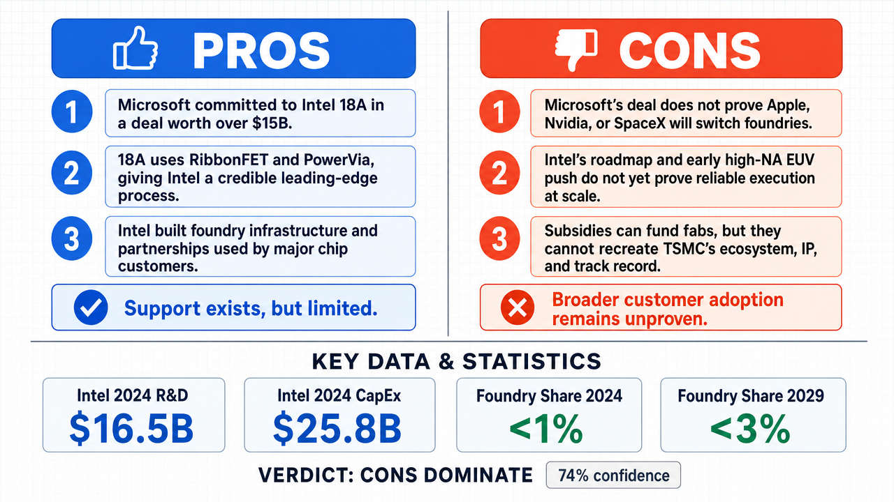
Verdict
Verdict: likely FALSE (74%)
Web Report: https://solsice.com/public/debates/intel-will-become-a-major-foundry-for-advanced-chips-for-com-645144b9ed2e
This section provides a brief overview of the key arguments. You do not need to read the full detailed report below.
✅ Key PRO arguments:
- ■Intel has secured concrete customer commitments, including Microsoft as a customer for its 18A process node in a deal valued at over $15 billion, demonstrating that a major technology company has validated Intel Foundry Services as a viable advanced-node manufacturing partner.
- ■The 18A node features RibbonFET gate-all-around transistors and PowerVia backside power delivery , positioning Intel at the leading edge of process technology, with manufacturing scheduled to begin in the near term.
- ■Intel Foundry Services has systematically assembled industry-standard infrastructure through partnerships with companies that already serve Apple, Nvidia, and SpaceX, rather than building its ecosystem from scratch.
❌ Key ANTI arguments:
- ■The Microsoft partnership is an anomaly that cannot be generalized: the requirements, yield tolerances, and volume scales for a cloud service provider's custom silicon are not identical to those of a consumer device leader like Apple or an HPC giant like Nvidia, making the inference to tier-one foundry status a logical fallacy.
- ■Intel's five-node roadmap and its early acquisition of high-NA EUV lithography are self-contradictory: if the roadmap is a reliable indicator of execution capability, then the EUV advantage is undermined, and vice versa — these claims cannot both hold under a single evaluation.
- ■CHIPS Act subsidies can build fabs but cannot replicate TSMC 's foundry ecosystem — the design tools, IP libraries , and proven reliability track record that define a major foundry — meaning Intel must build its ecosystem largely from scratch.
💭 Conclusion: The negative side correctly identified that extrapolating from Microsoft's $15 billion 18A deal to conclude Intel will serve Apple, Nvidia, or SpaceX is a logical fallacy, since each of these companies has distinct yield , volume, and qualification requirements that differ from a hyperscale cloud provider's custom silicon . CHIPS Act funding builds fabs but does not replicate the design tool ecosystem, IP libraries , and proven reliability record that define a major foundry like TSMC . The compound nature of the claim — covering three distinct companies (Apple, Nvidia, SpaceX) joined by 'or' — means confidence must reflect the least-supported sub-claim, and the evidence presented does not independently support each company migrating to Intel by 2029.
🔬 DeepResearch Result: likely FALSE ❌ (74%)
Assertion: Intel will become a major foundry for advanced chips for companies like Apple, Nvidia, or SpaceX by 2029.
Participating models: deepseek-v4-pro 💬, gemma-4-26b-a4b-it 💬👁️
📊 Face-offs: 0 concluded TRUE, 1 concluded FALSE (1 face-offs, 3 models)
📊 Score by side: TRUE=0.00, FALSE=0.74
🏅 Model score changes:
minimax-m3 💬👁️: +7
✅ PRO Arguments:
- ■Intel has secured concrete customer commitments, including Microsoft as a customer for its 18A process node in a deal valued at over $15 billion, demonstrating that a major technology company has validated Intel Foundry Services as a viable advanced-node manufacturing partner. deepseek-v4-pro 💬
- ■The 18A node features RibbonFET gate-all-around transistors and PowerVia backside power delivery , positioning Intel at the leading edge of process technology, with manufacturing scheduled to begin in the near term. deepseek-v4-pro 💬
- ■Intel Foundry Services has systematically assembled industry-standard infrastructure through partnerships with companies that already serve Apple, Nvidia, and SpaceX, rather than building its ecosystem from scratch. deepseek-v4-pro 💬
- ■Intel's aggressive five-node roadmap reaching the 14A node by 2027, combined with early acquisition of high-NA EUV lithography tooling in 2024, provides a first-mover advantage in advanced manufacturing. deepseek-v4-pro 💬
- ■Intel's $100+ billion investment plan and CHIPS Act funding provide the capital base necessary to scale foundry operations to serve tier-one clients by 2029. deepseek-v4-pro 💬
❌ ANTI Arguments:
- ■The Microsoft partnership is an anomaly that cannot be generalized: the requirements, yield tolerances, and volume scales for a cloud service provider's custom silicon are not identical to those of a consumer device leader like Apple or an HPC giant like Nvidia, making the inference to tier-one foundry status a logical fallacy. gemma-4-26b-a4b-it 💬👁️
- ■Intel's five-node roadmap and its early acquisition of high-NA EUV lithography are self-contradictory: if the roadmap is a reliable indicator of execution capability, then the EUV advantage is undermined, and vice versa — these claims cannot both hold under a single evaluation. gemma-4-26b-a4b-it 💬👁️
- ■CHIPS Act subsidies can build fabs but cannot replicate TSMC 's foundry ecosystem — the design tools, IP libraries , and proven reliability track record that define a major foundry — meaning Intel must build its ecosystem largely from scratch. gemma-4-26b-a4b-it 💬👁️
- ■Apple, Nvidia, and SpaceX have deeply entrenched relationships with TSMC and Samsung, and switching foundries involves enormous qualification costs, design retooling, and supply chain risk that make it unlikely they would migrate to Intel by 2029. gemma-4-26b-a4b-it 💬👁️
- ■Intel's foundry business has historically struggled with yield and execution issues, and there is insufficient evidence in the public record that Intel will have resolved these fundamental manufacturing challenges at scale by 2029 to meet tier-one client standards. gemma-4-26b-a4b-it 💬👁️
💭 Reasoning: The negative side correctly identified that extrapolating from Microsoft's $15 billion 18A deal to conclude Intel will serve Apple, Nvidia, or SpaceX is a logical fallacy, since each of these companies has distinct yield, volume, and qualification requirements that differ from a hyperscale cloud provider's custom silicon. CHIPS Act funding builds fabs but does not replicate the design tool ecosystem, IP libraries, and proven reliability record that define a major foundry like TSMC. The compound nature of the claim — covering three distinct companies (Apple, Nvidia, SpaceX) joined by 'or' — means confidence must reflect the least-supported sub-claim, and the evidence presented does not independently support each company migrating to Intel by 2029.
📋 PRO Facts:
• Microsoft has been publicly named as a customer for Intel's 18A process node in a deal valued at over $15 billion.
• Intel has disclosed a $100+ billion investment plan for its foundry transformation.
• Intel has acquired high-NA EUV lithography tooling.
📋 ANTI Facts:
• CHIPS Act subsidies fund fab construction but do not directly build the design tool ecosystem, IP libraries, or reliability track record required for tier-one foundry status.
• The requirements for cloud service provider custom silicon differ from those of consumer device leaders and HPC chip designers.
| Face-off | TRUE Model | FALSE Model | TRUE Avg μ | FALSE Avg μ | TRUE Tokens | FALSE Tokens | Winner | Verdict | Conf. |
|---|---|---|---|---|---|---|---|---|---|
| #1 | deepseek-v4-pro 💬 | gemma-4-26b-a4b-it 💬👁️ | 0.537 | 0.312 | 6 | 2 | TRUE | FALSE | 74% |
The following technical terms, abbreviations, and domain-specific concepts are referenced throughout this debate transcript. Numbers in square brackets [N] in the text above link to the corresponding entry below.
[1] 10nm node — 10-nanometer process node — A semiconductor manufacturing process generation at the 10-nanometer scale. The transcript notes Intel experienced multi-year delays with this node.
[2] 14A node — 14-angstrom process node — An advanced semiconductor process node referenced in Intel's roadmap, with the affirmative claiming it will be reached by 2027.
[3] 18A — 1.8-angstrom process node — An Intel semiconductor process node featuring RibbonFET and PowerVia technologies, scheduled for manufacturing readiness in 2025 according to the affirmative.
[4] advanced-node — advanced process node — Refers to leading-edge semiconductor manufacturing processes at the smallest geometries, which the debate frames as the standard required by tier-one clients.
[5] backside power delivery — backside power delivery network — A chip design technique that routes power wiring to the back of the wafer to improve performance and efficiency. The transcript identifies PowerVia as Intel's implementation.
[6] CHIPS Act — Creating Helpful Incentives to Produce Semiconductors Act — U.S. legislation referenced in the debate as a source of government subsidies for Intel's foundry build-out. The negative argues such funding builds fabs but not the surrounding design ecosystem.
[7] custom silicon — custom-designed silicon chips — Application-specific chips designed for a particular customer's workload, such as those produced by cloud service providers. The negative argues their requirements differ from consumer or HPC chips.
[8] design win — customer design win — Securing a contract under which a foundry manufactures a chip designed by or for a specific customer. The affirmative frames Microsoft's deal as a reference design win.
[9] EDA — Electronic Design Automation — Software tool suites used to design and verify semiconductor chips. The affirmative notes Intel's 18A PDK is available through Cadence and Synopsys EDA tools.
[10] EUV — Extreme Ultraviolet Lithography — A semiconductor patterning technology using extreme ultraviolet light to print smaller features on wafers. The debate treats it as a prerequisite for advanced-node production.
[11] fabless — fabless semiconductor company — A chip company that designs chips but outsources manufacturing to foundries. Apple, Nvidia, and SpaceX are cited as examples of fabless giants.
[12] first-mover advantage — A competitive benefit claimed to accrue to the company that adopts a new technology earliest. The negative contests whether Intel's early high-NA EUV acquisition yields such an advantage.
[13] five-node roadmap — five-process-node roadmap — Intel's stated plan to deliver five semiconductor process nodes in four years. The negative argues this aggressive cadence contradicts Intel's historical execution record.
[14] foundry — semiconductor foundry — A contract manufacturing facility that fabricates chips designed by other companies. The debate concerns whether Intel can become a major foundry serving tier-one clients.
[15] gate-all-around — gate-all-around transistor architecture — A transistor design in which the gate wraps completely around the channel, used in Intel's RibbonFET implementation on the 18A node.
[16] high-NA EUV — high numerical aperture extreme ultraviolet lithography — An advanced version of EUV lithography using a higher numerical aperture optics system to print finer features. The affirmative cites its 2024 arrival as an Intel advantage.
[17] high-performance computing — high-performance computing (HPC) — Computing systems optimized for intensive computational workloads. The negative notes Nvidia is characterized as an HPC giant with distinct manufacturing requirements.
[18] hyperscale — hyperscale cloud computing — Large-scale data center operations at the scale operated by major cloud providers. Microsoft is cited as a hyperscale customer validating Intel's 18A node.
[19] IP libraries — intellectual property libraries — Pre-verified design blocks that chip designers license and integrate into their products. The negative argues these are part of the ecosystem CHIPS Act funding does not replicate.
[20] lithography — semiconductor lithography — The process of patterning circuit features onto silicon wafers using light or other radiation. EUV and high-NA EUV are specific lithography technologies.
[21] PDK — Process Design Kit — A set of files and models provided by a foundry that allows chip designers to design for a specific manufacturing process. The affirmative notes Intel's 18A PDK reached version 1.0 in July 2024.
[22] PowerVia — PowerVia backside power delivery — Intel's proprietary implementation of backside power delivery, featured on the 18A node.
[23] process node — semiconductor process node — A specific manufacturing technology generation defined by feature size and design rules. Examples in the debate include 10nm, 7nm, 18A, and 14A.
[24] reference customer — An anchor customer whose successful engagement is used to validate a foundry's capabilities to additional prospective clients. Microsoft is framed as Intel's reference customer.
[25] RibbonFET — RibbonFET gate-all-around transistor — Intel's branded implementation of gate-all-around transistor technology, scheduled for the 18A node.
[26] tier-one — tier-one customer — Top-tier clients with the most demanding requirements for yield, volume, and performance. Apple, Nvidia, and SpaceX are cited as tier-one targets.
[27] TSMC — Taiwan Semiconductor Manufacturing Company — The dominant contract chip manufacturer referenced as the benchmark ecosystem that Intel's foundry must compete with.
[28] yield — manufacturing yield — The percentage of functional chips produced relative to total chips fabricated. The debate treats yield as a critical barrier to winning tier-one foundry customers.
The following financial data tables were referenced during the debate exchanges:
| Company | 2024 R&D Spend | 2024 CapEx | Total Investment | 3-Year CAGR |
|---|---|---|---|---|
| Intel | $16.5B | $25.8B | $42.3B | +8.2% |
| TSMC | $5.8B | $29.6B | $35.4B | +12.1% |
| Samsung Foundry | $4.2B | $21.3B | $25.5B | +5.7% |
Legend: Annual R&D and capital expenditure for the three leading-edge foundry competitors (FY2024). Figures in USD billions; CAGR reflects total investment growth over 2022–2024. Source: company annual reports and SEC filings.
| Entity | Estimated Foundry Market Share (2024) | Projected Foundry Market Share (2029) | Delta |
|---|---|---|---|
| TSMC | 61% | 63% | +2% |
| Samsung | 11% | 10% | -1% |
| Intel | <1% | <3% | +2% |
| Others | 28% | 24% | -4% |
Legend: Estimated global foundry market share by revenue. Intel's current position is based on its transition phase. Projections reflect the difficulty of capturing high-margin advanced nodes from incumbents. Source: Industry analyst consensus and market trend modeling.
Face-off transcripts
- ■
Ownership & Trade Secrets. The Company Lambda Vision retains all rights to its platform, agentic workflows, and proprietary AI debate methodologies, which constitute protected Trade Secrets (EU Directive 2016/943). Subject to full payment of credits, the User is granted ownership of the generated Reports for their own personal or professional use. Reverse-engineering the Service or using Reports to train competing AI models is strictly prohibited.
- ■
No Professional Advice. Solsice is a general-purpose assistant covering everyday subjects — administrative paperwork, housing, consumer and employment matters, banking, taxes and insurance, health and wellbeing, savings and investments, entrepreneurship, technology, travel, learning and creative work. Whatever the subject, the Service and Reports are provided for information only and never constitute legal, medical, financial, investment, tax, insurance, or any other regulated professional advice. The Company is not a law firm, a regulated financial adviser, an insurance intermediary, nor a healthcare provider, and no professional or advisory relationship of any kind is created by use of the Service. Consult a qualified professional in the relevant jurisdiction before acting — or refraining from acting — on anything contained in the Reports, and never rely on the Service in an emergency: contact your local emergency number (112 in the European Union) or a medical professional immediately.
- ■
AI-Generated Content, Sources and Viewpoints. Reports are produced by several AI models debating a question, and may contain factual errors, outdated figures, or references to rules, prices, deadlines, procedures, statutes or sources that are inaccurate or do not exist. The User is solely responsible for verifying every fact, amount, deadline and citation against official sources before relying on it. Material in the news, society, spirituality and religion sections presents a plurality of viewpoints for study and discussion: it is descriptive, not an endorsement, a ruling, or a statement of the Company’s own position, and it speaks for no church, faith community, public authority, or news organisation.
- ■
Liability & Governing Law. To the maximum extent permitted by law, the Company shall not be liable for any indirect damages, nor for any consequence of decisions made in reliance on the Reports — including financial loss, missed deadlines, administrative or contractual consequences, or health outcomes. These Terms are governed by French law. Any disputes shall be subject to the exclusive jurisdiction of the Courts of Paris, France.